As the world’s top-selling semiconductor seller, Intel not only develops chips, but also researches basic technologies for them. Intel’s Component Research division is presenting eight projects at the International Electron Device Meeting (IEDM 2021), from further scaled down CMOS transistors to 3D stacking processes and chips for quantum computers.

At Foverros Direct alias HBI, Intel makes direct contact with two stacked silicon dies with tiny copper tips
(Image: Intel)
Hybrid Bonding Interconnect (HBI)
While novel transistor structures such as Complementary FET (CFET) and 3D Gate All Around (GAA) FETs will only appear in series production after 2025 and magnetoelectric spin orbit (MESO) logic elements even later, Intel’s “Foveros Direct “aka Hybrid Bonding Interconnect (HBI) practically in front of the door. According to Intel, it could be used from the 7-nanometer production technology “Intel 4” or “Intel 3”.
At HBI, Intel packs two silicon chips directly on top of one another, with tiny copper contacts coming into contact with one another. According to Intel, this means that significantly more contacts per square millimeter are possible than with previous die-stacking processes that use tiny solder balls (bumps). AMD has already announced that it will have the “3D V-Cache” of the upcoming Epyc and Ryzen processors produced by TSMC using a similar process. The company Xperi also licenses one through its Tessera division “Direct Bond Interconnect” (DBI) or ZiBond.
ATM FET stack
Not only Intel, but also Samsung and TSMC will replace the field effect transistor (FET) with fin-shaped gate electrode (FinFET) that has been established for several years with upcoming production processes. Instead, nanoribbon, nanosheet and gate-all-around (GAA) FETs are used. The Intel version is called RibbonFET and should come after 2023 with the production technology “Intel 20A”.
In the manufacturing process for Complementary Metal Oxide Semiconductors (CMOS), which has been established for decades, one combines an n-channel and a p-channel MOSFET (NMOS / PMOS), usually side by side.
However, in order to save space, i.e. to put more transistors on the chip surface, Intel plans to stack them in the future. For the “Nanoribbon 3D Stacking”, Intel Component Research is experimenting with two methods: the construction of two functional layers one after the other (sequentially) with an insulating layer (silicon) oxide in between or the “self-aligned” structure directly on top of one another. Similar structures are also called Complementary FET (CFET).

MESO logic (left) may eventually replace CMOS; STMG uses moving magnetic domain boundaries.
(Image: Intel)
MESO logic
When all the CMOS stacks no longer help to continue Moore’s Law, the time for CMOS replacement strikes. That is why there have been lectures on carbon nanotubes (CNT) at semiconductor conferences for years.
Intel now reports on the first successful attempts with magnetoelectric spin-orbit (MESO) logic elements at room temperature, but writes itself that they “could possibly be produced in series”.
Another idea are spin-moment components that use the mobility of magnetic domain boundaries (Domain Walls, DW); Intel is cooperating with the European IMEC on research into a Spin Torque Majority Gate (STMG), a combination of logic and memory element.
Intel FeRAM

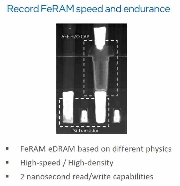
FeRAM cell with hafnium oxide
(Image: Intel)
A FeRAM memory cell that uses an antiferroelectric capacitor based on hafnium instead of a conventional capacitor structure could be closer to practical use. According to Intel, this means that it has measured very short access times of 2 nanoseconds and very high write resistance (endurance) in the range of 1 billion cycles. However, other manufacturers are also working on FeRAM, including FMC in Dresden.
Other innovations that Intel will be presenting at IEDM 2021 include the integration of high-performance gallium nitride (GaN) switching transistors on 300-millimeter CMOS wafers. This means that efficient voltage converters could be built directly into future processors.
In addition, Intel is experimenting with transition metal chalcogenides (TMD monolayers) such as molybdenum disulfide (MoS2) as a replacement for silicon in some places in semiconductors. This could make some structures even smaller.

(ciw)


