
Advertisement
The AI hype train continues to run at full steam and (not only) AMD wants to preserve its chances of getting as large a piece of this pie as possible. The company still expects a $150 billion market for accelerators in data centers – including graphics chips and FPGAs – in 2027. AMD reiterated this on Tuesday at the information event dubbed “Advancing AI” in San Jose, California.
To this end, AMD is now adding more salami slices to its Instinct MI300 accelerators, which were announced in mid-2022, shown for the first time at the beginning of the year and presented again in mid-2023, in terms of details and performance data. The MI300 should also perform well against Nvidia’s H100 and partly also GH200 due to the up to 192 GB memory. There are initially two versions of the MI300, the MI300X for the standard Open Accelerator Module (OAM) and the MI300A for the SH5 CPU socket. AMD is already delivering both to partners and, when asked about a CPU-only version, said “there is a chance” that this will come.

The AMD Instinct MI300 consists of 4 IO dies, 6 to 8 XCDs and 3 CCDs as well as the 8 HBM3 components and mechanical spacers
(Image: AMD)
Chiplets with 3D stacking


AMD showed the chips that are now available on site, even without heat spreaders. Here is a MI300X for the OAM format.
AMD manufactures both MI300 variants using chiplets, which are now also attached one on top of the other, i.e. using the 3D stacking process. The 2.5D packaging processes of earlier CDNA3, Ryzen and Epyc chips are also used. AMD calls the result 3.5D packaging. At the bottom there are four I/O dies (IOD), which not only connect the remaining chiplets, but also ensure the supply using through-silicon vias and 64 MB of infinity cache each as well as memory controllers for two HBM3 stack memories, a total of 256 MByte Infinifty Cache and 8 HBM stacks included. The IOD supplies each accelerator complex die (XCD) applied using a hybrid bonding process with up to 2.1 TByte/s of data, a total of 16.8 TByte/s across the entire MI300X.

AMD calls the complex packaging “3.5D”, even though strictly speaking it is of course only three dimensions.
(Image: AMD)
The IODs (and thus the applied logic chips) communicate with each other at 1.5 Tbyte/s on the long side and 1.2 Tbyte/s on the front side. With these data rates, you can at least pass memory access to remote controllers almost completely, albeit with sometimes increased latency (with two IOD jumps, since there is no cross connection). As if that wasn’t enough, the IODs also provide 8 × 16 lanes of the Infinity Fabric, half of which, i.e. 4 × 16, can also be used to connect PCI Express 5.0 devices. Each of these link groups can transfer 64 GB/s per direction. Four MI300A can be connected at 384 GB/s, eight MI300X reach 896 GB/s if you add up all seven external connections that remain after the x16 PCIe5 connection to the CPU. The approximately 13 × 29 millimeter chips are manufactured at TSMC using the inexpensive and proven N6 process.
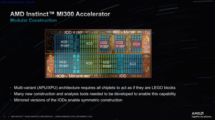
By rotating, but also mirroring, AMD assembles the MI300 like a terminal block.
(Image: AMD)
The logic chips are manufactured at TSMC using modern 5-nanometer technology and, unlike AMD’s 3D V-cache technology, are placed on top of the IODs so that the waste heat can be dissipated better. For the CPU cores with eight cores, each of which shares 32 MB of L3 cache, AMD uses the same CPU complex dies (CCDs) as in the Epyc 9004. The XCDs each contain 40 CDNA3 compute units, each of which However, two are switched off for economic reasons. An MI300X with eight XCDs therefore has 304 (active) compute units with 19,456 computing cores and 1216 special units for matrix multiplication.
Up to 750 watts and 32 percent faster than Nvidia H100
AMD states the Thermal Design Power (TDP) of the MI300X as up to 750 watts and showed performance values for the MI300A as up to 760 watts. However, since the accelerators work significantly faster than those of the previous generation, there is a net gain in efficiency when looking at the performance per watt. For densely populated matrices with INT8 accuracy, such as is often used in AI inferencing, i.e. the application of already trained models, MI300X delivers around 6.8x as much on paper with around 2.6 quadrillion operations per second (PetaOPS). Throughput like its predecessor MI250X and still 32 percent more than Nvidia’s current H100 SXM. The maximum clock rate required for this is 2100 MHz; the predecessor Instinct MI250X had to make do with 1700 MHz.
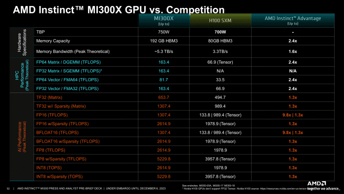
Tabular overview: MI300X versus Nvidia’s H100 SXM (without CPU part)
(Image: AMD)
The MI300X is designed as a pure accelerator within a classic rack server and is intended to deliver “Leadership AI Performance”, i.e. the highest performance for AI applications. The accelerator requires the help of a CPU such as AMD’s Epyc or Intel’s Xeon to boot, operate the OS and supply it. The MI300A swaps a quarter of the accelerator cores for 24 CPU cores based on Zen 4 from the Epyc 9004 and also works on its own. What’s more: Since the CPU and accelerator cores access the local memory together (“shared memory”), many time-consuming copying operations are no longer necessary and many algorithms can work much more efficiently and run faster.
AMD, on the other hand, sees the MI300A primarily in the area of high-performance computing and will, among other things, equip the upcoming 2-exaflops supercomputer El Capitan with it, as AMD’s Forrest Norrod confirmed once again.
Faster than Nvidia’s H100 thanks to 8 x HBM3
The MI300X boasts a whopping 153 billion transistors and 192 GB of HBM3 memory; AMD limited the MI300A with 146 billion transistors to 128 GB – because of the different application profile, said AMD. Nevertheless, each of the two has eight HBM3 stacks, only with capacities of 24 or 16 GB. An HBM3 stack delivers 665 GB per second and the entire package delivers a record-breaking 5.3 TB/s.

The connection of the computing units through the IO die with the HBM stacks is a science in itself. Instead of the CPU cores shown above, the MI300X has two additional XCDs here.
(Image: AMD)
The combination of memory size and transfer rate helps, among other things, some AI applications to achieve more performance, so that AMD sees itself well positioned against Nvidia’s established H100 accelerators. However, you only compare the MI300 against the H100 version with 80 GB; Nvidia has already announced those with 96 to 141 GB.
When it comes to inferencing AI applications, for example Flash Attention 2 or Llama2-70B, you are 10 to 20 percent ahead of Nvidia’s H100. According to AMD, in a server with eight accelerators, even larger large-language models like Bloom with 176 billion parameters have throughput values (tokens/s) that are up to 60 percent better than Nvidia’s H100 HGX. When it comes to AI training (Databricks MPT, 30 billion parameters), however, AMD only sees itself on a par with Nvidia’s offering. However, the more than twice as large memory means that two models could be trained at the same time (which would then be affected by the computing power) or twice as large, for example with 70 billion parameters instead of just 30.
The MI300A is intended to particularly excel in terms of efficiency and the advantages of shared memory access between the CPU and GPU cores. Compared to Nvidia’s H100, which communicates conventionally with its CPUs, AMD has a factor of 4 advantage if you use the HPC motorbike test of the OpenFOAM CFD simulation. Compared to Nvidia’s upcoming GH200, whose CPU and GPU parts can also access the memory together, AMD then draws a different comparison: In terms of theoretical computing throughput, they want to achieve twice the performance per watt and use Nvidia’s TDP specification of 1000 watts use the Grace Hopper superchip as a comparison.
Exciting: Not a single syllable was mentioned about Intel’s DataCenter GPU Max alias Ponte Vecchio.

Tabular overview: MI300A versus Nvidia’s H100 SXM (without CPU part)
(Image: AMD)
RocM 6 in December 2023
Without the right software, the best hardware is of no use. AMD had to experience this truism firsthand after Nvidia discovered the AI market very early on and captured it with numerous libraries and framework support for its in-house CUDA platform.
With MI300 they now want to expand the focus on open standards and the open source community. To do this, we are now working more proactively with AI software providers such as HuggingFace or the PyTorch framework.
In the course of December, AMD plans to release version 6 of the ROCm programming environment slash software platform. This should directly support MI300 and at least later also many of the modern Radeon GPUs that now have ROCm support, such as the RX 7900 XTX.
In a somewhat strange comparison, a performance advantage of factor 8 is given for a system with one MI300X with ROCm 6 versus ROCm 5 on four MI250s (without X!). The value refers to the inferencing latency of a Llama-2 model with 70 billion parameters. The comparison is strange because, in addition to new software versions, very different hardware is also used. The MI300X not only have 192 instead of 128 GB of memory, but can also consume 190 watts more (750 instead of 550 watts).
They were also able to bring OpenAI, the company behind ChatGPT, on board so that their upcoming 3.0 distribution Python-like programming environment Triton AMD’s Mi300 as well as other GPUs will be supported directly from the factory.
Note: AMD covered travel and hotel expenses for the author.
(csp)